Leading GaN & SiC Epi Wafer Manufacturer
Premium 4", 6", and 8" AlGaN/GaN on Si and GaN on SiC epitaxial wafers for high-frequency RF, power HEMT, and next-generation semiconductor applications. Trusted by global innovators since 2009.

This page is not the official website. Generated by AI, does not constitute any advice. If needed, please click here to visit the corresponding official website.
Premium 4", 6", and 8" AlGaN/GaN on Si and GaN on SiC epitaxial wafers for high-frequency RF, power HEMT, and next-generation semiconductor applications. Trusted by global innovators since 2009.

Established in 2009, Homray Material Technology (HMT) is a globally recognized leader in the development and manufacturing of wide-bandgap semiconductor materials, specializing in Gallium Nitride (GaN) and Silicon Carbide (SiC) wafers.
As a top-tier GaN epi wafer manufacturer, HMT delivers high-quality AlGaN/GaN on Si, GaN on SiC, and GaN on Sapphire epitaxial wafers. Our products are engineered for RF, power electronics, and optoelectronic applications, with optimized performance including extremely low buffer leakage and minimal trap density.
With a global footprint across Europe, the USA, Southeast Asia, and South America, HMT achieved over $65 million in sales in 2020. Our commitment to excellence, backed by ISO and CE certifications, ensures reliability and performance for next-generation semiconductor devices.
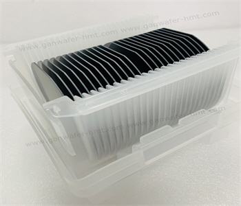
High-performance GaN and SiC epitaxial wafers engineered for RF, power, and HEMT applications. Available in 4", 6", and 8" diameters with customizable technical parameters.

AlGaN/GaN on Si and pGaN on Si epitaxy for next-gen power and RF electronics.
E-Mode Power HEMT structure for high-efficiency switching.

4" and 6" AlGaN/GaN on SiC epi wafers for high-frequency RF devices.

With SiN or GaN cap layer for enhanced device stability.
High-voltage power devices with excellent thermal management.
Normally-on devices with high efficiency and fast switching.
Optimized for microwave and millimeter-wave applications.
Free-standing GaN substrates in 2", 4", and square formats.
Engineered for performance, reliability, and scalability in next-gen semiconductor applications.
Optimized 2DEG mobility, low buffer leakage, and high breakdown voltage for superior device efficiency.
ISO and CE certified manufacturing processes ensuring consistent quality and reliability.
Serving partners in Europe, USA, Southeast Asia, and South America with fast delivery.
CMOS-compatible processes enable mass production and cost-effective scaling.
We offer GaN epitaxial wafers on Silicon (Si), Silicon Carbide (SiC), and Sapphire substrates, each optimized for specific RF or power applications.
Yes, we support customization of doping levels, thickness, and device structures for AlGaN/GaN and pGaN HEMT wafers based on customer requirements.
GaN on SiC offers superior thermal conductivity, higher power density, and better reliability for high-frequency RF applications like 5G and radar systems.
Yes, our GaN-on-Si technology is designed to be compatible with CMOS fabrication processes, enabling cost-effective mass production.
For inquiries, quotes, or technical support, visit our official website to connect with our team.
Visit Official Website to ContactTel: 15366208370
Email: kim@homray-material.com
LiSheng Industrial Building, 60SuLi Road, WuZhong District, JiangSu Province, P.R.China
Notice for Buyers: If you are a buyer, the above information is generated by AI collection and does not constitute any advice. If necessary, please visit the corresponding official website.
For Domain Owners: If you are the domain owner and do not want to be included by fobcompany.info, please contact support@fobcompany.info via your corporate email to cancel. We will cancel your inclusion within 3 business days.
如果您是域名所有者 不想被fobcompany.info收录 请用企业邮箱联系support@fobcompany.info 取消收录 我们将在3个工作日取消您的收录
Service Request: If you are other domain and want to be included, please contact support@fobcompany.info
如果您是其他域名合作 也请联系support@fobcompany.info